 | –≠–ª–µ–∫—Ç—Ä–æ–Ω–Ω—ã–π –∫–æ–º–ø–æ–Ω–µ–Ω—Ç: BYM11-400 | –°–∫–∞—á–∞—Ç—å:  PDF PDF  ZIP ZIP |

Vishay General Semiconductor
BYM11-50 thru BYM11-1000, RGL41A thru RGL41M
Document Number 88547
26-Jun-06
www.vishay.com
1
Surface Mount Glass Passivated Junction Fast
Switching Rectifier
FEATURES
∑ Superectifier structure for high reliability
condition
∑ Patented glass-plastic encapsulation technique
∑ Ideal for automated placement
∑ Fast switching for high efficiency
∑ Low leakage current
∑ High forward surge capability
∑ Meets environmental standard MIL-S-19500
∑ Meets MSL level 1, per J-STD-020C, LF max peak
of 250 ∞C
∑ Solder Dip 260 ∞C, 40 seconds
∑ Component in accordance to RoHS 2002/95/EC
and WEEE 2002/96/EC
TYPICAL APPLICATIONS
For use in fast switching rectification of power supply,
inverters, converters, and freewheeling diodes for
consumer, automotive and telecommunication.
MECHANICAL DATA
Case: DO-213AB, molded epoxy over glass body
Epoxy meets UL 94V-0 flammability rating
Terminals: Matte tin plated leads, solderable per
J-STD-002B and JESD22-B102D
E3 suffix for commercial grade, HE3 suffix for high
reliability grade (AEC Q101 qualified)
Polarity: Two bands indicate cathode end - 1st band
denotes device type and 2nd band denotes repetitive
peak reverse voltage rating
Patented*
Æ
DO-213AB
*Glass-plastic encapsulation
is covered by
Patent No. 3,996,602,
brazed-lead assembly to
Patent No. 3,930,306
MAJOR RATINGS AND CHARACTERISTICS
I
F(AV)
1.0 A
V
RRM
50 V to 1000 V
I
FSM
30 A
t
rr
150 ns, 250 ns, 500 ns
V
F
1.3 V
T
j
max.
175 ∞C
MAXIMUM RATINGS (T
A
= 25 ∞C unless otherwise noted)
PARAMETER
SYMBOL
BYM
11-50
BYM
11-100
BYM
11-200
BYM
11-400
BYM
11-600
BYM
11-800
BYM
11-1000
UNIT
FAST SWITCHING TIME DEVICE:
1ST BAND IS RED
RGL41A
RGL41B RGL41D RGL41G
RGL41J
RGL41K
RGL41M
Polarity color bands (2nd Band)
Gray
Red
Orange
Yellow
Green
Blue
Violet
Maximum repetitive peak reverse voltage
V
RRM
50
100
200
400
600
800
1000
V
Maximum RMS voltage
V
RMS
35
70
140
280
420
560
700
V
Maximum DC blocking voltage
V
DC
50
100
200
400
600
800
1000
V
Maximum average forward rectified
current at T
T
= 55 ∞C
I
F(AV)
1.0 A
Peak forward surge current 8.3 ms single
half sine-wave superimposed on rated load
I
FSM
30 A
Maximum full load reverse current, full
cycle average at T
A
= 55 ∞C
I
R(AV)
50 µA
Operating junction and storage
temperature range
T
J
, T
STG
- 65 to + 175
∞C
www.vishay.com
2
Document Number 88547
26-Jun-06
Vishay General Semiconductor
BYM11-50 thru BYM11-1000, RGL41A thru RGL41M
Note:
(1) Thermal resistance from junction to ambient, 0.24 x 0.24" (6.0 x 6.0 mm) copper pads to each terminal
(2) Thermal resistance from junction to terminal, 0.24 x 0.24" (6.0 x 6.0 mm) copper pads to each terminal
RATINGS AND CHARACTERISTICS CURVES
(T
A
= 25 ∞C unless otherwise noted)
ELECTRICAL CHARACTERISTICS (T
A
= 25 ∞C unless otherwise noted)
PARAMETER
TEST CONDITIONS
SYMBOL
BYM
11-50
BYM
11-100
BYM
11-200
BYM
11-400
BYM
11-600
BYM
11-800
BYM
11-1000
UNIT
Maximum
instantaneous
forward voltage
at 1.0 A
V
F
1.3
V
Maximum DC reverse
current at rated DC
blocking voltage
T
A
= 25 ∞C
T
A
= 125 ∞C
I
R
5.0
50
µA
Maximum reverse
recovery time
at I
F
= 0.5 A, I
R
= 1.0 A,
I
rr
= 0.25 A
t
rr
150
250
500
ns
Typical junction
capacitance
at 4.0 V, 1 MHz
C
J
15
pF
THERMAL CHARACTERISTICS (T
A
= 25 ∞C unless otherwise noted)
PARAMETER
SYMBOL
BYM
11-50
BYM
11-100
BYM
11-200
BYM
11-400
BYM
11-600
BYM
11-800
BYM
11-1000
UNIT
Maximum thermal resistance
R
JA
R
JT
75
(1)
30
(2)
∞C/W
ORDERING INFORMATION
PREFERRED P/N
UNIT WEIGHT (g)
REFERRED PACKAGE CODE
BASE QUANTITY
DELIVERY MODE
RGL41J-E3/96
0.114
96
1500
7" Diameter Plastic Tape & Reel
RGL41J-E3/97
0.114
97
5000
13" Diameter Plastic Tape & Reel
BYM11-600-E3/96
0.114
96
1500
7" Diameter Plastic Tape & Reel
BYM11-600-E3/97
0.114
97
5000
13" Diameter Plastic Tape & Reel
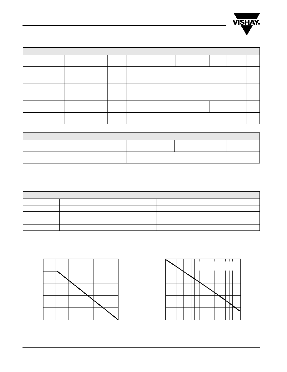
Figure 1. Forward Current Derating Curve
A
v
erage
F
or
w
ard
Rectified
C
u
rrent
(A)
25
50
75
100
125
150
175
0
0.25
0.5
0.75
1.0
1.25
Resistive or
Inductive Load
Terminal Temperature (∞C)
Figure 2. Maximum Non-Repetitive Peak Forward Surge Current
1
10
100
0
10
15
20
25
30
Number of Cycles at 60 Hz
P
eak F
o
r
w
ard S
u
rge C
u
rrent (A)
T
j
= T
j
max.
8.3 ms Single Half Sine-Wave

Document Number 88547
26-Jun-06
www.vishay.com
3
BYM11-50 thru BYM11-1000, RGL41A thru RGL41M
Vishay General Semiconductor
PACKAGE OUTLINE DIMENSIONS in inches (millimeters)
Figure 3. Typical Instantaneous Forward Characteristics
Figure 4. Typical Reverse Characteristics
0.4
0.6
0.8
1.0
1.2
1.4
1.6
0.01
0.1
1
10
Instantaneous Forward Voltage (V)
Instantaneo
u
s F
o
r
w
ard C
u
rrent (A)
T
j
= 25 ∞C
Pulse Width = 300 µs
1 % Duty Cycle
0
20
40
60
80
100
0.01
0.1
1
10
Percent of Rated Peak Reverse Voltage (%)
Instantaneo
u
s Re
v
erse C
u
rrent (
µ
A)
T
j
= 100 ∞C
T
j
= 25 ∞C
Figure 5. Typical Junction Capacitance
Figure 6. Typical Transient Thermal Impedance
1
10
100
1
10
100
Reverse Voltage (V)
J
u
nction Capaci
tance (pF)
T
j
= 25 ∞C
f = 1.0 MHz
V
sig
= 50 mVp-p
0.01
0.1
1
10
100
0.1
1
10
100
Mounted on 0.20 x 0.27" (5 x 7 mm)
Copper Pad Areas
T
r
ansient Ther
mal
Impedance
(∞C/
W
)
t - Pulse Duration (s)
SOLDERABLE ENDS
1st BAND
0.022 (0.56)
0.018 (0.46)
0.205 (5.2)
0.185(4.7)
D1 =
0.105
0.095
(2.67)
(2.41)
D2 = D1
+ 0
- 0.008 (0.20)
D2
0.022 (0.56)
0.018 (0.46)
DO-213AB
0.138 MAX
(3.5) MAX
0.049 MIN
(1.25) MIN
0.118 MIN
(3.0) MIN
0.238 (6.0)
REF
Mounting Pad Layout
1st band denotes type and positive end (cathode)

Legal Disclaimer Notice
Vishay
Document Number: 91000
www.vishay.com
Revision: 08-Apr-05
1
Notice
Specifications of the products displayed herein are subject to change without notice. Vishay Intertechnology, Inc.,
or anyone on its behalf, assumes no responsibility or liability for any errors or inaccuracies.
Information contained herein is intended to provide a product description only. No license, express or implied, by
estoppel or otherwise, to any intellectual property rights is granted by this document. Except as provided in Vishay's
terms and conditions of sale for such products, Vishay assumes no liability whatsoever, and disclaims any express
or implied warranty, relating to sale and/or use of Vishay products including liability or warranties relating to fitness
for a particular purpose, merchantability, or infringement of any patent, copyright, or other intellectual property right.
The products shown herein are not designed for use in medical, life-saving, or life-sustaining applications.
Customers using or selling these products for use in such applications do so at their own risk and agree to fully
indemnify Vishay for any damages resulting from such improper use or sale.